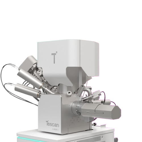
Tescan AMBER X™ 2 is an advanced plasma FIB-SEM that combines the Mistral™ Plasma FIB column with the field-free BrightBeam™ UHR SEM to deliver high speed, precision, and versatility in sample preparation and characterization.
Designed for advanced materials science research, it enables Ga⁺-free, low-damage, fully automated TEM lamella preparation with TEM AutoPrep Pro™, while supporting high-throughput 2D and 3D multimodal analysis.
- A unified platform for both precision TEM prep and large-volume 3D characterization
- Ga+-free TEM lamella preparation with minimal amorphization damage
- Fully automated (TEM AutoPrep Pro™) workflow for consistent and accessible sample preparation
- High-throughput 3D analysis with stable beam performance at all FIB and SEM currents
- Field-free BrightBeam™ UHR SEM for magnetic, non-conductive, and sensitive materials
- Energy-filtered electron signals for enhanced surface and phase contrast of the samples
Where Tescan AMBER X™ 2 makes the difference
High-Precision, Large-Area Cross Sections
Generate high-quality cross sections at high milling currents with Mistral™ Plasma FIB, combining rapid material removal with nanometer-scale accuracy for both large-volume and fine-detail workflows.
Ultra-High-Resolution Nanocharacterization
Image and analyze the widest range of materials with the BrightBeam™ field-free UHR SEM, delivering stable low-energy performance ideal for magnetic, non-conductive, and beam-sensitive samples.
Ga+-Free TEM Sample Preparation
Prepare clean, damage-reduced TEM lamellae using Xe+ plasma FIB—achieving the precision of Ga+ workflows without the risk of gallium contamination.
Fast, Artifact-Reduced Large-Volume 3D Analysis
Accelerate large-area cross-sectioning and 3D tomography up to 1 mm while maintaining superior surface quality. The TESCAN Rocking Stage minimizes curtaining, even in porous, brittle, or highly heterogeneous materials.
Multimodal 3D Chemical and Structural Insight
Acquire EDS, EBSD, and ToF-SIMS data within a single FIB-SEM tomography workflow to reveal morphology, crystallography, elemental composition, and isotopic chemistry in true 3D.
Automated TEM Workflow Acceleration
Leverage TEM AutoPrep Pro™ for guided or fully automated lamella preparation. Region selection, geometry setup, and final polishing are streamlined, increasing reproducibility and freeing instrument time for imaging and analysis.
Scalable, User-Friendly Operation for Any Lab
Operate confidently with guided automation, intuitive controls, and modular Tescan Essence™ software—supporting both expert and novice users in high-throughput, multi-user environments.
Tescan AMBER X™ 2
Technical specification
|
Electron Optics
|
|
|
Electron Beam Column
|
BrightBeam™ Field-Free UHR-SEM Column
|
|
Electron Beam Resolution
|
|
|
Magnification
|
6x to 2,000,000x
|
|
Electron Source
|
Schottky field electron emitter
|
|
Electron Beam Landing Energy Range
|
50 eV – 30 keV (< 50 eV with BDM)
|
|
Probe Current
|
2 pA – 400 nA (continuosly adjustable)
|
|
Ion Optics
|
|
|
Ion Beam Column
|
Mistral™ Plasma Focused Ion Beam Column
|
|
Ion Beam Resolution
|
10 nm @ 30 keV
|
|
Maximum Field of View
|
1 mm @ 30 keV
|
|
Probe Current
|
1 pA – 3.3 uA
|
|
Ion Beam Energy Range
|
500 eV – 30 keV
|
|
Detectors
|
|
|
Standard Detectors
|
|
|
Optional Detectors
|
|
|
Analyzers
|
|
|
Stage & Sample
|
|
|
Stage
|
Motorized, 5-axis compucentric stage
|
|
X & Y axis travel range
|
130 mm
|
|
Z axis travel range
|
96 mm
|
|
Rotation
|
Compucentric, 360° (continuous)
|
|
Tilt range
|
Compucentric, -70° to +90°
|
|
Max. specimen height
|
92 mm (133 mm without stage rotation)
|
|
Max. specimen size
|
180 mm diameter with full XY moves, rotation, no tilt (larger samples possible with limited stage travel and rotation)
|
|
Maximum specimen weight
|
|
Tescan Amber X™ 2 Applications
- Tescan AMBER X™ 2 in Materials Science
- Tescan AMBER X™ 2 in Semiconductors
- Tescan AMBER X™ 2 in Batteries
- Tescan AMBER X™ 2 in Life Science (Large-volume processing, deep ROI access, and multimodal analysis of biological samples)